NVIDIA H100: Breaking Down H100 GPUs and Servers
Description: This report examines NVIDIA's H100 chip and server architecture, focusing on improvements in tensor performance, memory, and cooling that elevate AI workload efficiency and scalability.
- H100
- GPU
- Node
- Server
- Infiniband
- Supermicro
- Dell
Abstract
This report provides an in-depth breakdown of the NVIDIA H100 chip and server architecture, emphasizing their roles in advancing AI workloads. It details the H100's Hopper architecture, which brings substantial improvements in tensor core performance, memory bandwidth, and power efficiency, crucial for handling the intensive demands of large language models (LLMs). The report also examines the structure of multi-GPU server nodes, covering components like NVLink interconnects, memory systems, and cooling mechanisms that together enable efficient scaling and support high-compute AI infrastructure. Through this analysis, the report illustrates how the H100 chip and server architecture together set new benchmarks in AI efficiency and scalability.
GPU Primer
Why GPUs Are Essential for AI Tasks
Before diving deep into the core components of the H100 chip, it is essential to first understand GPUs, what they are composed of, and why they are necessary for AI workloads.
Limitations of CPUs
Central Processing Units (CPUs) are optimized for sequential processing and general-purpose tasks. They have a limited number of cores, making them inefficient for the highly parallel computations required in training and running large language models (LLMs). This leads to longer processing times and less efficient handling of the massive datasets involved in AI workloads.
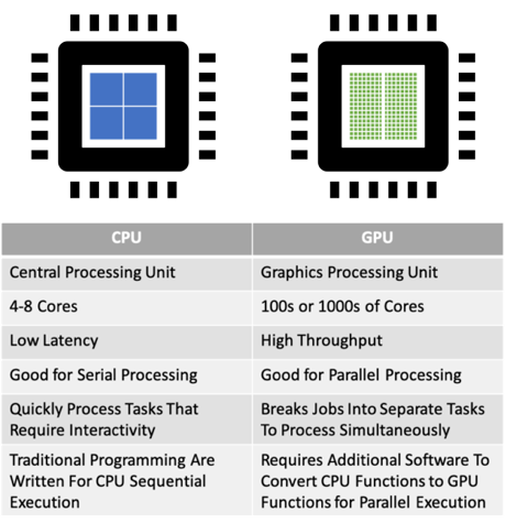
Where GPUs Excel
Graphics Processing Units (GPUs), originally built for graphics rendering, are specialized hardware accelerators whose parallel processing architecture excels at handling vast amounts of simultaneous calculations.
Graphics Processing Units (GPUs) are engineered for parallel processing with thousands of cores, allowing them to perform multiple calculations simultaneously.
This makes GPUs ideal for AI operations:
- Massive Parallelism: Accelerates computations by handling numerous operations at once.
- Optimized for Deep Learning: Specialized Tensor Cores enhance performance for neural network tasks.
- High Memory Bandwidth: Enables rapid data access, reducing bottlenecks during training and inference.
- Scalability: GPUs can be interconnected via NVLink (more on this later) to form powerful multi-GPU systems, essential for large models.
What Makes up a GPU Chip
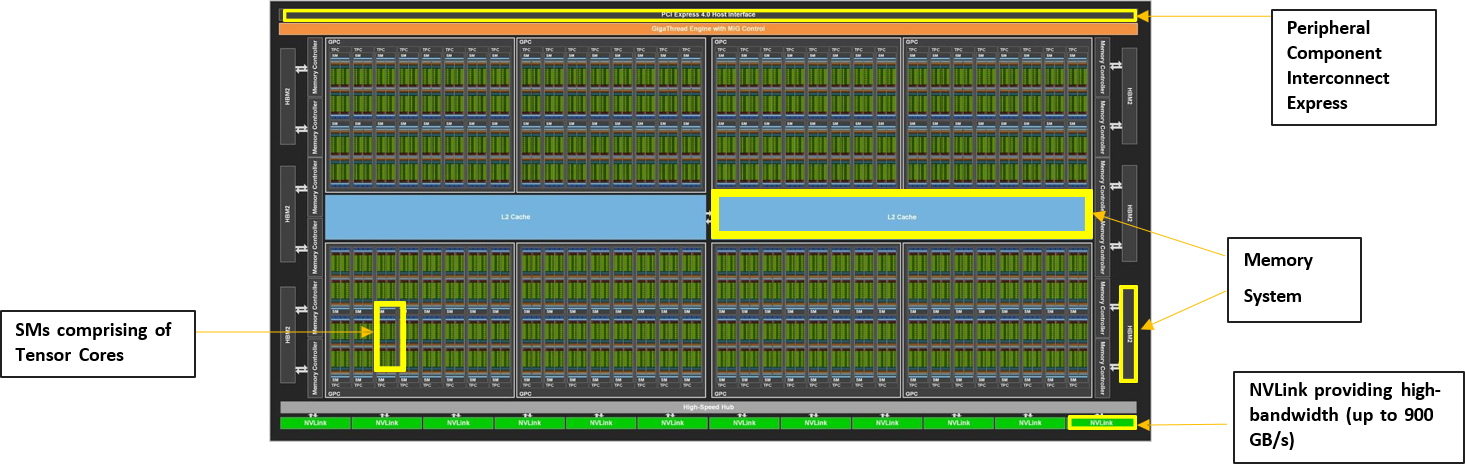
Processing Units:
- Streaming Multiprocessors (SMs): Primary processing blocks containing thousands of CUDA cores and Tensor Cores for parallel computation
- CUDA Cores: General-purpose processing units executing parallel calculations across thousands of threads
- Tensor Cores: Specialized units optimized for AI/ML matrix operations, crucial for accelerating neural network computations
Memory Hierarchy:
- Registers and shared memory for immediate data access within SMs
- L1/L2 caches for frequently accessed data
- High-Bandwidth Memory (HBM) providing massive bandwidth for data-intensive operations
Communication Infrastructure:
- NVLink interfaces for GPU-to-GPU connections
- PCIe: high-speed interface standard used for connecting (CPU-GPU communication here)
Control Systems:
- Memory controllers managing data flow between cores and memory
- Instruction dispatch units scheduling computational tasks
- Clock and power management optimizing performance and efficiency
Important Facts about the GPU
Why is NVLink needed?
NVLink is a high-speed interconnect by NVIDIA that enables rapid data transfer between GPUs and CPUs. It offers significantly higher bandwidth and lower latency than traditional methods, crucial for training large language models (LLMs). NVLink ensures efficient scaling across multiple GPUs by providing fast, low-latency communication, reducing bottlenecks, and accelerating both training and inference.
SXM v/s PCIe (comparing for the H100 Chip)
| Feature | PCIe | SXM |
|---|---|---|
| Compatibility | Standard Servers | High-Performance Computing (HPC) Servers |
| Memory | 80 GB | 80 GB |
| GPU Memory Bandwidth | 2 TB/s | 3.35 TB/s |
| Power Consumption (TDP) | 350W | Up to 700W |
| Target Applications | High-Throughput Data Analytics, Medical Imaging, Interactive Design and Visualization | Large-Scale AI Model Training and Inference on Massive Datasets, Drug Discovery, and Materials Science |
H100
The Hopper Architecture
The H100 GPUs were announced in 2022 to address the limitations of A100, and provide even more powerful and efficient solutions for quicker training for bigger models.
H100 advancements over its previous generation
- Hopper Architecture: Leverages the Hopper architecture, which brings significant improvements in tensor operations, memory bandwidth, and overall system efficiency.
- Fourth-Generation Tensor Cores: These new Tensor Cores offer enhanced performance for AI and machine learning workloads, including support for new data types and instructions.
- Improved Power Efficiency: The H100 GPUs are designed to be more power-efficient than A100
- Enhanced Interconnects: Supports advanced interconnects like NVLink 4 and InfiniBand, ensuring low-latency and high throughput communication between nodes.
- Increased Memory: Comes with larger memory capacity, including up to 80GB of HBM3 memory, crucial for handling large models and datasets.
H100 vs A100
| Specification | A100 | H100 |
|---|---|---|
| Architecture | Ampere | Hopper |
| Release Time | 2020 | 2022 |
| Networking | NVLink: 600 GB/s PCIe Gen4: 64 GB/s | NVLink: 900 GB/s PCIe Gen4: 128 GB/s |
| CUDA Cores | 6912 | 16986 |
| Highest TDP | 400W (lower) | 700W (higher) |
| GPU Memory | 80 GB HBM2e | 80 GB HBM3e |
| Memory Bandwidth | 2039 Gbps | 3.35 Tbps |
| FP64 Performance | 9.7 TFLOPS | 34 TFLOPS |
| FP64 Tensor Core Performance | 19.5 TFLOPS | 67 TFLOPS |
H100 Data Center
A Lot More Than Just the Chip
Modern AI models like GPT-4 have billions of parameters that demand massive computing power. One GPU can't handle this alone. A server node compromises around 8 GPUs that work together like a single powerful unit through high-speed connections. But even this isn't enough for training huge models or serving millions of users, so we need multiple server nodes in racks. This hierarchical structure (GPU → server node → rack → datacenter cluster) efficiently manages the extreme computing, power, and cooling needs of AI workloads. We will dive into the inner components of a GPU server node in this report.
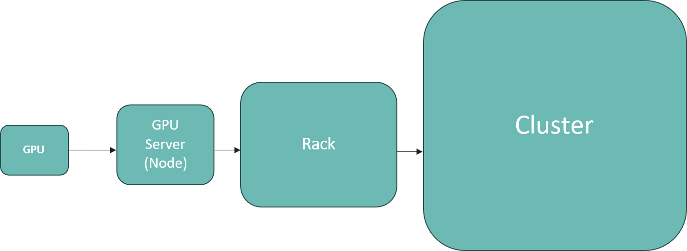
GPU
A single H100 chip
Server Node
Complete computing unit containing CPUs, GPUs, memory, and networking components that work together to process AI workloads.
Rack
A rack is a standardized frame (usually 42U tall) that organizes multiple chassis vertically with shared power distribution and networking.
Cluster
A cluster is a collection of networked racks that function as one unified computing system, allowing multiple servers to work together on massive AI workloads.
H100 Server
The Computing Brain of AI
We will now break down the main components that makes up a single GPU server node. In a GPU server node, the chassis is the physical framework that houses and organizes internal components like GPUs, CPUs, power supplies, and storage devices. It provides structural support and facilitates cooling airflow, ensuring all components are secure and properly cooled.
- CPU: Manages system operations and user requests, working with GPUs for efficient workload management.
- GPUs: Execute parallel computations required for AI and data-intensive tasks.
- High-Bandwidth Memory (HBM): Provides rapid data access for GPU computations, crucial for high performance.
- RAM: Temporarily stores data for quick CPU access, supporting multiple user sessions.
- Storage: High-speed SSDs and NVMe drives that securely store large datasets and minimize data access times.
- Cooling Systems: Include fans and heat sinks to maintain optimal temperatures and ensure reliability under heavy workloads.
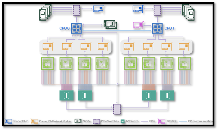
H100 Server
The Computing Brain of AI (cont.)
- Network Interfaces: High-speed connections like Ethernet or InfiniBand for efficient data transfer and remote access.
- Interconnects (NVLink): Enable fast communication between GPUs, reducing latency in multi-GPU workloads.
- PCIe: High-speed interface connecting GPUs and peripherals to the motherboard, providing necessary bandwidth.
- NVSwitch: NVIDIA Specific PCIe that is much faster and can connect nodes to enable faster communication between GPUs at scale.
- Power Supply Units (PSUs): Supply stable power to all components, handling high power demands.
What are the various types of Nodes?
H100 DGX vs HGX
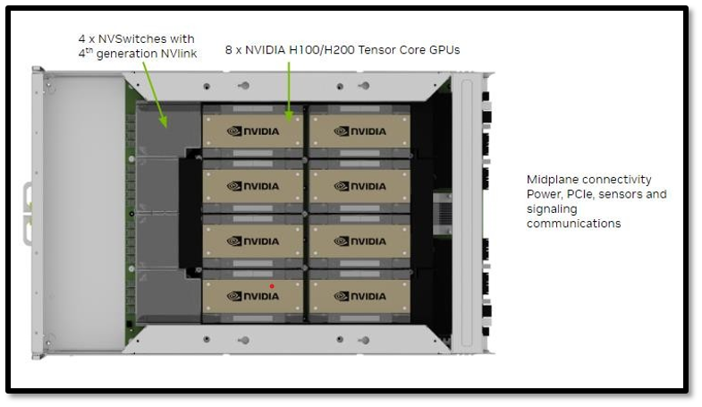
As defined previously a node is a server unit housed on a rack in the data center. It typically consists of 4 or 8 H100s along with CPUs, Storage and Networking/ Interconnect ports allowing it to communicate with the rest of the cluster. It is a modular unit allowing for easier expansion.
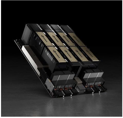
- NVIDIA DGX H100: NVIDIA's template for an ideal H100 datacenter node, featuring 8 H100 SXM GPUs, dual Intel Xeon 8480C CPUs, 4 NV Switches, and support for up to 400Gb/s InfiniBand/Ethernet, with a 10.2kW TDP. It's non customizable, set directly by NVIDIA as a template for certified chassis makers.
- NVIDIA HGX H100: Built by NVIDIA certified manufacturers like Dell, Supermicro, and HPE, these servers also use H100 SXM GPUs but offer customizable options, such as 4-GPU configurations, Intel or AMD CPUs, and power efficiency tweaks, allowing for flexibility in networking and power needs compared to the fixed DGX.
There are additional H100 Node types for smaller tasks:
- NVIDIA EGX: This is even more modular, it features the grace hopper superchip (H100 GPU + CPU in one chip) The focus is power efficiency and modularity for smaller workloads.
- NVIDIA MGX: This is the server based on the PCIe version of the h100 with various configurable networking, cooling and CPU options. This is the lowest cost option.
H100 Server Manufactures
What is Best for You?